When light and electrons shine together
›Spasers‹: the smallest lasers in the world

Over the past 20 years, semiconductor nanowires have evolved into flexible devices in optoelectronics, where they are now used as light-emitting diodes (LEDs), in photovoltaic cells and in other areas. They can also be used as tiny lasers: The incident light is reflected at the facet ends of the wire, which is approximately 200 nanometres thick, and is amplified as it passes through, thus creating a laser. As it stands, lasers made of semiconductor nanowires are the smallest in the world – but they could be even smaller…
By Sebastian Hollstein
Prof. Dr Carsten Ronning and his team of physicists at the Institute of Solid State-Physics are working with Prof. Dr Thomas Pertsch from the Institute of Applied Physics to investigate a new method that could be used to produce lasers with even smaller diameters. In this method, the semiconductor nanowires only serve as a source of light and a tool. Their project, which is entitled ›Nonlinear dynamics in plasmonic hybridized semiconductor nanowires‹, is being carried out at the ›Nonlinear Optics down to Atomic Scales‹ collaborative research centre (NOA CRC).
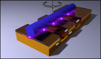
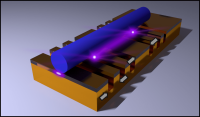
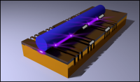
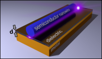
The scientists’ approach involves placing a semiconductor nanowire on a metal surface, which is separated by a dielectric intermediate layer that is less than ten nanometres thick. »When the wire and metal are excited with light, a so-called spaser is created in the intermediate layer«, explains Carsten Ronning. »This phenomenon is caused by the oscillation of different waves. While the semiconductor nanowire produces what is known as an optical mode, a wave of light particles, the electrons also oscillate in the metal and form a plasmonic mode«. Both waves react with each other in the intermediate layer and create a hybrid mode.
Once the incident light has been amplified in this field, it acquires the properties of a laser – a plasmonic laser or ›spaser‹. With a diameter of only five to ten nanometres, however, the spaser is significantly smaller than the light beam emitted by the semiconductor – and much faster and more intense.
As part of the project, the researchers are attempting to manipulate the spaser’s properties in a targeted manner by altering various parameters, particularly by defining the qualities of the plasmonic nanostructures on the substrate. If these structures are modified, the light can be captured more strongly within individual points. The substrate also allows the researchers to manipulate the frequency and wavelength, which should have an impact on the speed and intensity of the laser.
That’s why Ronning and his team are first focusing on the structure of the substrate. »As part of their bachelor’s dissertations, young researchers and Francesco Vitale, a doctoral candidate involved in this project, have drafted various schemes and developed a method with which we can write the necessary structures on the substrate. Other researchers have been focusing on how to place the semiconductor nanowire in certain positions on the substrate,« explains Ronning. »As we’re working on the nanoscale, these processes are extremely complicated. We’ve even bought a special tool – a nanoManipulator – to place the wires onto the surface and move them around in a targeted manner«. More set screws are required due to various factors, such as the higher intensity of the spaser. This produces nonlinear effects which, among other things, enable the light to change colour.
As the project progresses, the team will be looking to gather more information as to what happens inside the field between the semiconductor and metal. Thanks to the spectroscopic measurements carried out by Thomas Pertsch, the physicists are able to observe how quickly and how far the wave that becomes a spaser is propagated. Such valuable information helps to functionalize the mini laser and thereby explore its potential for various applications.
»The range of applications is generally very broad, because microelectronic components are also getting smaller, such as microchips in smartphones,« explains Carsten Ronning. »This type of laser is a highly promising step towards developing optical-based chips that would be able to transfer data even faster, because light moves faster than electrons«. In addition, the spaser could be used as a spectroscopy unit on a ›lab on a chip‹ (i.e. on tiny analysis tools for chemical and biological investigations).
By working with scientists from other specialist fields at the collaborative research centre, the laser experts will be able to further explore the range of potential applications, such as to enable the spectroscopy of a single protein.
Nano-sized cones, pyramids and rings made of metals are tiny optical antennas. Such as radio or television antennas, optical antennas can also be used to capture, focus and emit electromagnetic waves. The length of the antenna is adapted to the wavelength of the electromagnetic radiation. While radio waves have a wavelength of several metres, the wavelength of visible light varies from only 380 to 780 nanometres. In other words, optical antennas have to be extremely small.
When plasmonic nanostructures are illuminated, the electromagnetic light waves interact with the moving conduction electrons in the metal. The electrons start to oscillate collectively and propagate themselves; these oscillations are referred to as ›surface plasmon polaritons‹ (or ›plasmons‹ for short). As a result, much smaller structures can be illuminated and detected than with the original incident light and the Abbe diffraction limit can be bypassed.